
|
Home
| pfodApps/pfodDevices
| WebStringTemplates
| Java/J2EE
| Unix
| Torches
| Superannuation
|
| About
Us
|
|
|
Build a Basic uC Led Driver
|
by Matthew Ford 17th June 2008 (revised 29th June
2008)
© Forward Computing and Control Pty. Ltd. NSW
Australia
All rights reserved.
This tutorial describes the construction and programming of a
basic pulse width modulator controlled linear current regulator for
driving a LED at 500mA.
No SMD devices are used.
You
can use this same basic design for supplying up to 5A or more by
changing the current sense resistor.
See also: Bluetooth
Controlled Led Driver - A Tutorial and Android
Controlled LED Driver
Construction time 2hrs.
The
tutorial covers
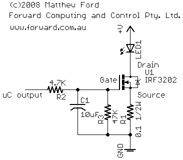
The circuit for this basic uC (micro Controller) controlled LED driver is
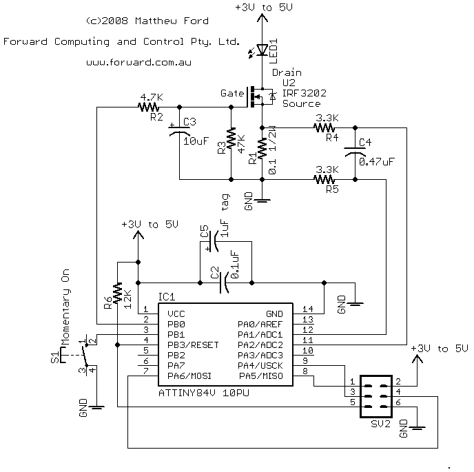
The circuit shown above can be powered from 3 x NiMH batteries or 1 Lithium-Ion battery (or even 3 Alkalines). The uC will work all the way down to 1.8V which is below the fully discharged level of the batteries.
The basic operation of the controller is as follows:-
R1 (0.1ohm) is the current sense resistor. The uC measures the voltage across this resistor to determine the current flowing in the led. If the current is below the required level the uC controller sets the uC output to +5V which charges C3 through R2 raising the gate voltage on the FET U2 this lowers the Fet's resistance and increase the current through the led. IRF3202 is an N-Channel fet which turns on as its gate voltage is increased compared to is source pin. When the current exceeds the required level the uC controller set the uC output to 0V and the discharges C3 so lowering the voltage on the Fet's gate and so increasing the Fet's resistance and reducing the current though the Led.
R3 is there to make sure the Fet gate has zero Volts (i.e. Fet is OFF) when the control uC circuit is powered down.
R2 and R3 form a voltage divider from the uC output to ground which limits the maximum voltage that can be applied to the gate of the Fet. With the values shown the maximum fet gate voltage is about 4.55V.
This is called BangBang control and is simple and effective. The capacitor, C3 smooths out the square wave output from the uC so the Fet gate sees only a small ripple.
R4, R5 and C4 form an RC filter for the current sense voltage applied to the uC differential Analog to Digital 10 bit converter. The uC has an internal gain of x20 applied to this signal and then converts the differential voltage to a count between 0 and 1023, where 1023 equals 1.1V (approximately). Dividing 1.1V by the internal gain of 20 implies that full range on the input to the uC is about 55mV. With a sense resistor of 0.1ohm this means full range current is 55/0.1 = 550mA. Of course you can change the full range current by changing the sense resistor.
C2 and C5 are supply filtering for the uC and R6 is the Reset pull-up resistor.
The
parts list is:-
Part Value
C2   0.1uF ceramic
C3   10uF tag
C4   0.47uF
C5   1uF tag
IC1  ATTINY84V 10PU
LED1 K2 LUMILED + heatsink
R1   0.1 1/2W
R2   4.7K
R3   47K
R4   3.3K
R5   3.3K
R6   12K
S1   Momentary On
SV2  6PIN HEADER
U2   IRF3202
Veroboard with copper tracks on the back
500mA power pack 3 to 12V selectable
For programming the uC you need
  AVR Studio 4 software (free download, discussed below)
  AVR Dragon (about $50) or other programmer
  6pin header cable
  USB cable + Windows2000/XP/Visa computer
As you can see from the photo my sense resistor (0.1 ohm) is a 5W resistor. Only a 1/2W resistor is needed but this was what I had to hand. The uC is an Atmel Attiny84V 10PU. Note the V suffix this indicates the low voltage part which will run down to 1.8V. The Led heat sink I used was CPU self adhesive heat sink. If you use a normal heat sink you will also need some thermal epoxy to attach the led to the heatsink. My heatsink is a bit small for 500mA continuous. If you want to run at 500mA all the time you need a larger heatsink, i.e. one at least twice a big.
The AVR Studio 4 provides the code compiler and runs the AVR Dragon programmer. You can download AVR Studio 4 from www.atmel.com (as at July 2008 the direct link is http://www.atmel.com/dyn/Products/tools_card.asp?tool_id=2725 scroll down to the Software section and choose AVR Studio 4.14). AVR Dragon is available from Digiky (and others) in the US and Avnet in Australia. There are other software compilers available that run under Linux (google avr programmer linux).
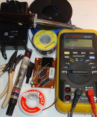
Other items you need are a fine tipped soldering iron (20W is OK), some solder and a multimeter and tools. I also suggest solder wick and a flux pen.
The power pack's output voltage is selectable from 3V to 12V.
Do
not select an output voltage above 4.5V as the normal maximum running
voltage for the uC is 5V.
After 2hrs work I had this
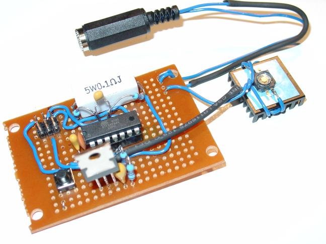
The only messy part is the 6 pin header which did not fit neatly into the layout of the copper tracks on the back of the veroboard. I had to cut away some track connections to wire the header up.
Before inserting the uC, plug in the power pack and check the voltage at pin 1 and 14 of the uC. Pin 1 should be +Volts. Also check Pin 4 for +Volts and pin 2 of the 6 pin programming header. Double check the connections and orientation of the 6 pin programming header.
The uC's I use are from the Attiny series by Atmel. This design uses the Attiny84V which has 8K of programmable memory, 512 bytes of EEPROM and 512 byte of RAM.
I use a very basic program flow, shown below

This uses only one interrupt, the ADC conversion complete interrupt. It has the advantage of simplicity and low noise since there is no processing or output pin changes while the ADC conversion is running. It has the disadvantage of reducing the sampling rate of the ADC since all the input and output processing is done each ADC cycle. However my present code still has a sampling rate of about 5300 samples/sec which is more than enough for controlling a torch.
The Attiny84 has a number of built in timers. I don't use any of these. Instead I run my own counters from the ADC loop to generate timers of 1/100 sec and 1/10sec and 1/2sec. Because the ADC loop times vary depending on the processing being done these timers are only approximate but appear to be with in +/- 5%.
An outline of the code is shown below
//---- MAIN PROGRAM --------------------------------------------
.org 0x0000
   rjmp RESET
.org    ADCCaddr//      = 0x000b        ; ADC Conversion Complete
   rjmp  ADC_INT
RESET:
// initialize uC here
...
  sei  // enable interrupts
E_LOOP:
    // set up for ADC conversion and then sleep
  ldi Temp, (1<<SM0) | (1<<SE)
  out MCUCR, Temp   // ADC noise reduction rest zero, enable sleep
  sleep     // goto sleep this starts the ADC
  // wake up on ADC interrupt
  // on completion of interrupt returns here
  rjmp E_LOOP  // loop for next ADC
//----END MAIN PROGRAM --------------------------------------------

//----HANDLE ADC INTERRUPT -------------------------------------------------
ADC_INT:
    // save ADC results
    in ADCLow,ADCL
    in ADCHigh,ADCH
.....
// process the ADC measurement of current, voltage, etc
.....
// all paths jmp to here
END_ADC_INT:
   rcall SWITCH_DEBOUNCE  // every ADC cycle about 5kHz
   rcall INCREMENT_100HZ_TIMER  // may set volts or temp flag
   rcall PROCESS_STATE_TRIGGERS
reti  // return from interrupt, interrupts enabled here
//----END ADC_INT -------------------------------------------------As a first attempt, the code in BasicLedDriver.asm just controls the current in the led to a fixed setpoint. It does not used the pushbutton. The led is always on when the power is applied. You could use this in a simple on/off torch by just switch the battery on and off.
To compile this code, download the AVR Studio 4 from www.atmel.com (as at July 2008 the direct link is http://www.atmel.com/dyn/Products/tools_card.asp?tool_id=2725 scroll down to the Software section and choose AVR Studio 4.14). Start a new project
(todo fill in details here)
To follow the code you need to refer to know what the instructions mean. The on-line help in AVR Studio provide explanations of the instructions. You will also need to refer to the attiny24/44/84 data sheet the details of meaning of various control register bits.
There are 4 main sections in the code
Definitions. These dot commands include a file of “standard” definitions for this uC and define (.equ) some useful names for constants and registers (r16,r18,r19)
.include "tn84def.inc"
.equ CURRENT_SP = 1000  // the current setpoint, 1000 = full scale current, approx 500mA
.equ SW_B = PB1  // define name for switch input pin
.equ uC_OUTPUT_B = PB0  // define name for uC output pin
.def Temp = r16// Temporary register
.def ADCLow = r18 // low byte of adc
.def ADCHigh = r19 // high byte of adc
Interrupt Vectors. These dot org commands place relative jump (rjmp) instructions at particular locations in the program memory. On Reset. when the power comes up or when the Reset input pin is allowed to go high, the uC automatically goes to location 0x0000 and executes the instruction found there. Here we jump to our RESET label. When the ADC conversion completes its interrupt jumps to the location 0x000d and from there jumps to our ADC_INT label
.org 0x0000
   rjmp RESET
.org ADCCaddr  // = 0x000d      ; ADC Conversion Complete
   rjmp  ADC_INT
Main Program. The main program initializes the uC, set up the ADC and then sleeps waiting for the ADC to complete it conversion
The first part prevents this code being interrupted by any other interrupt and then sets the uC internal clock to 4Mhz. The default is 1Mhz set by the programming fuses. 4Mhz is the fasted you can run this uC when the supply is less then 2.7V. Next pin PB0 is set as an output, to drive the Fet, and its state is set to 0V, by default all pins are inputs. The same code applies a pullup resistor to the PB1 pin, the Switch input. This pullup resistor insures the input is held high when the switch is open.
Then the ADC is setup. You need to set its clock frequency to <200KHz to get full accuracy, by dividing the main uC clock. It is also enabled and its interrupt is enabled by this code. The ADMUX register controls which input pins the ADC is connected to and what the reference voltage is and the input gain. Here we are using the internal 1.1V reference and applying a gain of 20 to the differential measurement between PA2 and PA1 inputs.
Finally the interrupts are enabled again before setting the uC into low noise ADC conversion mode. The sleep command starts the conversion. When it completes the ADC interrupt jumps to our ADC_INT label. When it returns here, the command after the sleep just loops and starts another conversion.
RESET:
    cli  // disable interrupts
    // set clock to 4Mhz so can run down to 1.8V
    ldi Temp, (1<<CLKPCE)
    out CLKPR, Temp  // enable clock change for next 4 cycles
    ldi Temp, (1<<CLKPS0) // divide by 2 for 4Mhz clock
    out CLKPR,Temp  // set 4Mhz clock

    // uC_OUTPUT_B (PB0) is an output for driving the led  DDB0=1, PB0=0 low OFF to start
    // SW_B (PB1) is the switch input  DDB1=0, PB1=1 with pullup
    ldi Temp,(1<<SW_B)
    ldi r17, (1<<uC_OUTPUT_B)
    out PORTB,Temp
    out DDRB,r17

    // Enable ADC
    ldi Temp, (1<<ADEN) | (1<<ADIE) | (1<<ADPS2) | (1<<ADPS0)
    // (1<<ADEN) enable ADC
    //  ADSC zero do not start conversion yet
    //  ADATE zero do not trigger conversion
    //  (1<<ADIE) enable ADC interrupt need I-bit in SREG set also
    //  (1<<ADPS2) (1<<ADPS0) pre-scale for 4Mhz clock and <200Khz ==> >20 pre-scale say 32
    //   i.e. 1,0,1  for 4Mhz/32 = 125Khz
    out ADCSRA, Temp       // set the  ADCSR

    // set Vref 1.1V (1,0) and the ADC mux inputs and gain (101101) PA2+ve, PA1-ve, x20
    ldi Temp, (1<<REFS1) | (1<<MUX5) | (1<<MUX3) | (1<<MUX2) | (1<<MUX0)
    out ADMUX, Temp

    sei  // enable interrupts
E_LOOP:
    // set up for ADC conversion and then sleep
    ldi Temp, (1<<SM0) | (1<<SE)
    out MCUCR, Temp   // ADC noise reduction rest zero, enable sleep
    sleep     // goto sleep
    // wake up on ADC interrupt
    // on completion of interrupt returns here
    rjmp E_LOOP  // loop for next ADC
ADC Interrupt Handler This is where the program jumps to each time the ADC finishes a conversion. First collect the results of the 10 bit conversion into the two registers ADCLow, ADCHigh. Then do a double word subtraction of the CURRENT_SP. First subtract the low bytes. The Carry flag is set if the absolute value of the low byte of the CURRENT_SP is larger then the absolute value of ADCLow. Then the high bytes are subtracted including this carry flag also. Finally if the result is >=0 then branch to the CURRENT_HIGH label else drop through to the CURRENT_LOW branch. As described in the circuit description above if the current is high then make the output low (0 volts). If the current is low then make the output high (+V). The reti command returns from the interrupt handler.
//-------------------------------------
//  ADC interrupt, result available
//-------------------------------------
ADC_INT:
  // save ADC results
  in ADCLow,ADCL
  in ADCHigh,ADCH

  subi ADCLow, low(CURRENT_SP)
  sbci ADCHigh, high(CURRENT_SP)
  brge CURRENT_HIGH      // branch if ADC >= setpoint  (signed comparison)
  // else ADC < setpoint

CURRENT_LOW:
  // ADC < setpoint  ==> make output high
  sbi  PORTB, uC_OUTPUT_B   // set output high
  rjmp END_ADC_INT

CURRENT_HIGH:
  // ADC > setpoint  ==> make output low
  cbi  PORTB, uC_OUTPUT_B   // set output low
  rjmp END_ADC_INT

// all paths jmp to here
END_ADC_INT:
reti  // interrupts enabled here
//----END ADC_INT -------------------------------------------------
AVRStudio4 is used to write, compile and debug the uC code. The AVR Dragon board is used to write the compiled code to the Attiny84 and to debug the code in circuit. AVRStudio4 requires a Window2000/XP/Vista PC to run it. A USB connection is required to connect to the AVR Dragon programming board.
First download and install AVRStudio4 (V4.14 or later from www.atmel.com). When the installation is complete, re-run the install program and select Modify, and then tick to install the USB driver
![]()
Once the drive has finished installing, connect the AVR Dragon to a USB port. It will be found by the operating system. After a while the “Please Wait ..” dialog will dissappear. The AVR Dragon board has now been installed.
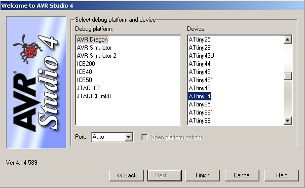
Start AVRStudio4 and click on the New Project button. Select Project type as Atmel AVR Assembler and type in the project name.

Click Next and on the next panel select AVR Dragon and Attiny84
Click Finished. When the Project opens, choose from the menu item Tools -> AVR Dragon Upgrade and upgrade the AVR Dragon's firmware. This will close the current project. When the upgrade is complete, open your BasicLedDriver project and copy the code for BasicLedDriver into the BasicLedDriver.asm file.
Choose the menu item Build -> Build to compile the code. There should be no errors or warnings.
Connect the AVR Dragon ISP 6pin header to the 6pin header on the circuit board.
If you cannot found a ready made 6pin header cable, you can make your own. Construction time 5mins.
Buy some ribbon cable, 6 strands or more, and two insulation displacement headers 6pin (or 10pin). Strip back the ribbon cable to 6 strands and place in the header, aligning the red stripe on the pin 1 side of the header plug.

Here
I am using a 10pin header. The circled mark is the pin 1 marker.
Then squeeze the header together in a vice and add the locking clip (if there is one). Do the same for the other end of the cable. Finished. Plug in your cable, aligning the red stripe with the pin 1 marking on the board headers.
Apply 3V to your Led Driver board.
NOTE: When tesing and debugging your code do not exceed 3V on the Led Driver board. This will protect your led from being burnt out if the uC output gets stuck on High, turning the FET hard on.
Now choose Tools -> Program AVR -> Auto Connect to open the AVR programming dialog. When this first runs it will probably not work. This is due to the ISP Frequency being to high for your circuit. Click Settings button and set the frequency to 125Khz and Write it.
The ISP mode should be automatically set. Check that the Device is Attiny84. You should now be able to Read the Signature of your uC.

If you still have problems such as an ISP Mode Error dialog box, the press F1 while the error dialog is open to get help on what else could be wrong. (Is the power to the board off??)
On the Fuses tab, set the following Fuse settings and click the Program button. You can check them by clicking the Verify or Read buttons.

Leave the other tabs with their default values.
You are now ready to write your code the uC. You have already build the code so there should be .hex file in the same directory as the .asm file. You need to specify this file as the Input HEX file on the Progam tab.

Make sure the Supply Voltage is set to 3V, then click on the Flash Program button to write the compiled code to your in circuit uC. The led should come on when the programming is finished.
Measure the voltage across the 0.1 ohm sense resistor. I measured about 20mV. That is I = V/R = 20mV/0.1ohm = 200mA. With a 3V supply there is not enough supply voltage to drive the led at 500mA. If you measure the voltage across the FET Drain to Source you should find only a few millivolts as the uC output should be turning the FET hard on trying get the led current up to 500mV. Measure the voltage from the Gate of the FET to ground. You should get about 0.9 x the supply volts (i.e. around 2.7V for a 3V supply. The 0.9 factor is due the voltage divider R2, R3. The voltage at the Gate is equal to the supply voltage x R3/(R2+R3) = supply voltage x 0.909
If everything looks OK so far, you can try setting the voltage to 4.5V. First attach the multimeter across the 0.1 ohm sense resistor. Then while watching the multimeter, turn the supply on. The multimeter should read about 50mV (45mV to 55mV), if the multimeter reads >60mV then the uC is not controlling the current in the led. Turn the supply off and check your circuit for shorts. When I shorted the Drain to the Source of my FET, I read 90mV across the sense resistor, i.e. 900mA with a 4.5V supply voltage.
With a 4.5V supply, the FET Gate voltage in my circuit was about 1.9V. This indicates that the uC is switching its output on and off to control Gate voltage and hence the FET's resistance and hence the current in the led. Measure the voltage from the FET's Drain to Source. My measurement was about 0.95V. This indicates the FET's resistance is being controlled to R = V/I = 0.95V/0.5A = 1.9ohms. You can watch this Drain Source voltage vary as the led heats up. As the led heats up, the uC continues to adjust the FET's resistance to keep the current through the led constant.
The possible variation in sense resistor voltage of between 45mV and 55mV is primarily due to range of uC's ADC 1.1V reference voltage. The 1.1V reference voltage can be anywhere between 1.0V and 1.2V If the ADC reference voltage is higher then the current will be higher for the same ADC conversion count. The voltage across the sense resistor will also vary due to the accuracy of the 0.1 ohm resistor. Plus or minus 5% is typical. All these variations are not critical. However if the current is too high you can always just reduce the setpoint in the code. If the current is too low, you will need to reduce the sense resistor. Putting a 1ohm resistor in parallel with it will reduce it by about 10% and hence increase the full range current level by 10%.
Note: You will not get an accurate measurement of the current by using your multimeter as a current meter unless there is still enough voltage for the uC to regulate the led current to the setpoint. This is because your multimeter meter has its own sense resistor which drops some of the supply voltage. To see if the uC is still regulating the current in the led, you need another multimeter to measure the FET Gate voltage at the same time and check that it is less then 0.9 times the supply voltage.
Now that your circuit is running, you can try some of the other programs in this tutorial or code your own, however remember to set the Flash Input HEX File to the same name as the .asm file you have just compiled. Opening a new project does not automatically update the Input HEX file setting, you need to do this yourself.
The AVR Studio4 allows you simulate the program and single step through it. However using the AVR Dragon you to debug the code in the uC while it is running in your test circuit. It does this by using three wires, VCC, GND and Reset (debugWIRE).
Make sure the Supply Voltage is set to 3V. When debugging, the program will be paused and so will not be controlling the current to the led. A 3V supply prevents the led from burning out.
1) To Start debugging, first compile and load the program into the uC (see above).
2) Choose the menu item Debug -> Select Platform and Device and select AVR Dragon and Attiny84. You need to do this step even after you selected these when setting up the project.

You
are now ready to start debugging the code in the uC in your test
circuit.
3) Then select the menu item, Debug -> Start Debugging. You will see the following dialog.
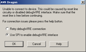
Choose
“Use SPI to enable debugWIRE interface” and click OK.
This brings up the following dialog
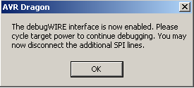
Clicking
OK brings up the following dialog

Click
Retry to enter Debug mode. All this is the same as setting the DWEN
flag via the ISP Flags tab.
4) The program will stop at the first instruction. The rjmp to the RESET label.

The
I/O view on the right hand side allows you to inspect and directly
change any of the uC control registers.
Use Debug -> Single
Step Over, (F10) to step through the code.
Stop at the sei
instruction just before the E_LOOP: label.
Expand the PORTB
I/O
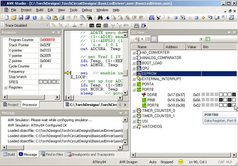
You
can see that the DDRB 0 bit is set, making this pin an output. Click
on the PORTB 0 bit to set it. The led comes on. Click it again to set
it to zero, the led goes off.
Leave PORTB 0 set, i.e. led on.
Scroll the code window to the
ADC_INT: label and set a breakpoint on the first instruction
after the ADC_INT label using the menu item, Debug ->
Toggle Breakpoint.
Then select Debug->Run. The code stops at
the breakpoint. You can now inspect the AD_CONVERTER ADC value
0x0103. Right click on the window and un-tick the Hexadecimal
Display.

This
then shows the ADC count (and every other value in the window) in
decimal, i.e. 259 counts out of 1023. That is about 140mA

The
reference voltage in the uC is 1.1V (+/-0.1V). Dividing by the 20x
gain of the differential input gives 55mV full scale across the
0.1ohm resistor. That is a full scale current of 0.55A =
0.055V/0.1ohm. So 259 counts out of a full scale of 1023 is
0.55*259/1023 = 139mA
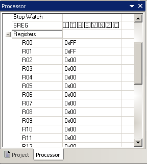
As you single step through the ADC_INT: code you can hover your mouse over the register variables to view their values and the names. On the left hand side you can expand the Registers node and view and directly change the value of the any register.
You
can also change/correct the code on the fly and continue running or
restart the program. The AVR Studio4 will automatically compile and
reload the uC through the AVR Dragon debugWire interface.
So you can see the debug modes available are very powerful. Explore the other features for yourself.
When you are finished debugging you may want to get back into ISP mode. You cannot un-tick the ISP DWEN flag because the ISP programming does not work while debugWIRE is enabled.
To get out of debugWIRE.
Select the menu item Debug ->
Start Debugging.
Then when debugging has started a new menu item
is added to the bottom of the Debug menu, AVR Dragon Options.
Select
the new menu item Debug -> AVR Dragon Options. This brings up the
following dialog

Click on the Disable debugWIRE button, which bring up the following dialog

Clicking
YES, exits debugWIRE and re-enables ISP and bring up the confirmation
dialog

Finally
click OK and close the AVR Dragon dialog.
You can now access Tools -> Program AVR -> Auto Connect to open the AVR programming dialog and change the fuse settings, lock bits, program the uC etc. using the ISP programming interface.
So now you have a constant current led driver that is switched on and off by turning the power on and off. But there is a push button on the board. What about controlling the led using the push button. Press to turn on, press to turn off.
A naive approach to this is to just read the input the switch is connected to using the instructions
    sbic PINB, SW_B   // read SW if SW high jump to released
    rjmp SW_HIGH_RELEASED
    // else drop through to SW_LOW_PRESSED
However it turns out this is not reliable. When switches open and close the contacts tend to bounce and give a number of fast open and closes before the switch settles out to its final state. See Guide to Debouncing for more details.
That article contains some code for debouncing switches. The code presented here is not as compact but is easier to follow and includes a switch changed trigger. The full code is in SwitchedLedDriver.asm . Below is the debounce code.
The SWITCH_DEBOUNCE is called after each ADC conversion, i.e. About 5000 times pre sec. First it clears the SW_SwitchChanged flag. This flag is only set for the single cycle during with the switch changed state, after allowing for debounce. Next it increments the DEBOUNCE_counter. This counter counts from 0 to 253. It is limited at 253 to prevent it wrapping round and triggering extra SwitchChanged triggers. Next the switch input is checked to see what the current state of the switch is. The code then jumps to the appropriate label. The actions are similar so lets just look at SW_LOW_PRESSED.
SW_LOW_PRESSED first checks the last input state. If the last input was also low then the code jumps to check for debounce. If the last input was high then the switch input has just changed and the code drops through to update the last input and clear the debounce counter.
SW_low_check_debounced checks the current DEBOUNCE_counter against the Debounce_Count_Low value (about 10mS) if they are not equal then the code just returns. If the count equals the debounce value then the SW_SWDown flag is set to indicate the switch is down (debounced) and the SW_SwitchChanged flag is set to indicate the switch state has just changed.
SW_HIGH_RELEASE preforms similar checks for when the switch is released.
// Debounce Counter Counts allows up to 50mS debounce = 250 count
.def DEBOUNCE_Counter = r17 //  count debounce timeout
.equ Debounce_Count_Low = 50 // about 0.01 sec  = 50x5kHz
.equ Debounce_Count_High = 50 // about 0.01 sec  = 50x5kHz
// increase the count if you switch needs a longer debouce in one direction

//------------------------------------------------
//SW_Flags,  Holds the current debounced switch state and last state and change trigger
//------------------------------------------------
.def SW_Flags = r20  // 0b00000000 initially i.e. Switch up and last switch up and not trigger and led off
.equ SW_SWDown = 0   // bit0, 1 if button pressed, 0 if button released.
.equ SW_SWLastInput = 1  // bit1,  1 if last read SW pressed (low) not debounced
.equ SW_SwitchChanged = 2 // bit2, 1 if switch just changed else 0
.equ SW_LedOn = 3 // bit3, 1 if led is on, 0 if off
//------------------------------------------------
.......
SWITCH_DEBOUNCE:
    andi SW_Flags, ~(1<<SW_SwitchChanged) // clear switch changed flag

    cpi DEBOUNCE_Counter, 0xfe    // inc counter but limit to 253
    brsh DEBOUNCE_Counter_LIMITED  // skip increment if at or above limit
    inc DEBOUNCE_Counter ; count up 5KHz counter for debouce

DEBOUNCE_Counter_LIMITED:
    sbic PINB, SW_B   // read SW if SW high jump to released
    rjmp SW_HIGH_RELEASED
    // else drop through to SW_LOW_PRESSED

SW_LOW_PRESSED: // read SW low/pressed
    sbrc SW_Flags, SW_SWLastInput //check if last flag high/on, rjmp if was high
    rjmp SW_low_check_debounced   // if last input low and this one low check for debounce low

    // else this sw low and last high, set last input to high and reset debounce counter
    ori SW_Flags,(1<<SW_SWLastInput)  // 1 for last pressed
    clr DEBOUNCE_Counter;  load counter restart counter for next debounce
    rjmp SWITCH_DEBOUNCE_RETURN // no change yet

SW_low_check_debounced:
    cpi DEBOUNCE_Counter, Debounce_Count_Low
    brne SWITCH_DEBOUNCE_RETURN  // only do switch change on DEBOUNCE count
    // else update output and return
    ori SW_Flags,(1<<SW_SWDown) // debounced
    ori SW_Flags, (1<<SW_SwitchChanged) // debouced switch changed
    rjmp SWITCH_DEBOUNCE_RETURN

SW_HIGH_RELEASED: // read SW high/released
    sbrs SW_Flags, SW_SWLastInput  // check if last flag low/off, rjmp if was low
    rjmp SW_high_check_debounced  // if last input high and this one high check for debounce high

    // else this sw high and last low, clear last input and reset debounce counter
    andi SW_Flags,~(1<<SW_SWLastInput)
    clr DEBOUNCE_Counter;  load counter restart counter for next debounce
    rjmp SWITCH_DEBOUNCE_RETURN  // no change yet

SW_high_check_debounced:
    cpi DEBOUNCE_Counter, Debounce_Count_High
    brne SWITCH_DEBOUNCE_RETURN  // only do switch change on DEBOUNCE count
    // update output and return
    andi SW_Flags,~(1<<SW_SWDown) // debounced
    ori SW_Flags, (1<<SW_SwitchChanged) // debouced switch changed
    rjmp SWITCH_DEBOUNCE_RETURN

SWITCH_DEBOUNCE_RETURN:
ret
So now we have our debounced input. We need a few more changes to get the get the led to turn on and off. First in the ADC_INT code we add at the top a test to see if the Led should be on or off. If it should be off we always set the uC output to low to drive the Fet off. Otherwise we let the current control do its work.
At the bottom of the code we add calls to our SWITCH_DEBOUNCE code to update the switch input flags and then to a PROCESS_STATE_TRIGGERS procedure to handle changes in the switch state. The new ADC_INT code is
ADC_INT:
    // save ADC results
    in ADCLow,ADCL
    in ADCHigh,ADCH

    sbrs SW_Flags, SW_LedOn // skip rjmp if led should be on
    rjmp CURRENT_HIGH  // if led off set output low
    // else led should be on
    subi ADCLow, low(CURRENT_SP)
    sbci ADCHigh, high(CURRENT_SP)
    brge CURRENT_HIGH      // branch if ADC >= setpoint  (signed comparison)
    // else ADC < setpoint

CURRENT_LOW:
    // ADC < setpoint  ==> make output high
    sbi  PORTB, uC_OUTPUT_B   // set output high
    rjmp END_ADC_INT

CURRENT_HIGH:
    // ADC > setpoint  ==> make output low
    cbi  PORTB, uC_OUTPUT_B   // set output low
    rjmp END_ADC_INT

// all paths jmp to here
END_ADC_INT:
   rcall SWITCH_DEBOUNCE  // every ADC cycle about 5kHz
   rcall PROCESS_STATE_TRIGGERS
reti  // interrupts enabled here
The PROCESS_STATE_TRIGGERS code is responsible for updating the SW_LedOn flag in response to switch presses. The code is straight forward
PROCESS_STATE_TRIGGERS:

    sbrs SW_Flags, SW_SwitchChanged   // skip rjmp is there was a switch change
    rjmp END_PROCESS_STATE_TRIGGERS   // no switch change so just finish

    // else switch changed state, set SW_LedOn accordingly
    sbrs SW_Flags, SW_SWDown // skip rjmp if switch is down/on
    rjmp END_PROCESS_STATE_TRIGGERS  // do nothing on switch relase
    // else toggle led on state
    sbrc SW_Flags, SW_LedOn // skip rjmp if led already off
    rjmp TURN_LED_OFF   // led on, so turn off
    // else turn led on
    ori SW_Flags,(1<<SW_LedOn) // turn on
    rjmp END_PROCESS_STATE_TRIGGERS // finished

TURN_LED_OFF:
    andi SW_Flags,~(1<<SW_LedOn) // turn off
  // drop through to end

END_PROCESS_STATE_TRIGGERS:
ret
If there has been no switch change then just return. Otherwise if the new switch state is On/down then toggle the LedOn flag.
Finally a note on setting the Debounce_count_high and low. You can check this will an oscilloscope by outputing the SW_SWLastInput flag to a spare uC pin and measure the bounce in your particular switch. However another way that does not require an oscilloscope is to just try it. If the led always reliablely turns on and off then the debounce counts are long. If not make them a bit longer and try again. If you get to 50mS (about 250 counts) without success then buy a different switch.
Now that you have the push button working, you can use it to switch the led between multiple levels, Off, Low, Med, High. To provide an extensible bases for further development I will use Torch States as opposed to flags to implement these levels. The full code is in ThreeLevelDriver.asm
.def Torch_State = r22   // initially 0 == off
.equ Torch_State_OFF = 0  // the torch state constants
.equ Torch_State_LOW = Torch_State_OFF+1 // 1
.equ Torch_State_MED = Torch_State_LOW+1 // 2
.equ Torch_State_HIGH = Torch_State_MED+1 // 3
.equ Torch_State_EXCEEDED = Torch_State_HIGH+1 // this and higher states invalid
While you can easily write a program to handle three levels by using flags, you will find that as you controller becomes more complex States are the way to go. The torch is switched between states by triggers. In this case the trigger is the push button changing from up to down. Once the new state of the torch is set then the new state can be use to set the appropriate current setpoint for the ADC_INT: procedure.
In order to vary the setpoint, it is now stored in two registers, SP_High and SP_Low, and the ADC_INT code changes to
    sub ADCLow, SP_low
    sbc ADCHigh, SP_High
The PROCESS_STATE_TRIGGERS first sets the New_TORCH_State to the current TORCH_State and then determines the New_TORCH_State depending on the triggers, if any. It there are no triggers then we just return from PROCESS_STATE_TRIGGERS, otherwise the New_TORCH_State is set and then at the end it is transferred to become the current TORCH_State and the new current setpoint loaded depending of the TORCH_State. See the code file ThreeLevelDriver.asm for details.
//-------------------------------------
//PROCESS_STATE_TRIGGERS
//-------------------------------------
PROCESS_STATE_TRIGGERS:
   mov New_TORCH_State, TORCH_State // set initial state

   cpi TRIGGER_Flags, 0  // are any trigger flags set
   breq END_PROCESS_STATE_TRIGGERS   // all zero so just return

   sbrs TRIGGER_Flags, TRIGGER_SwitchChanged
   rjmp Finished_SwitchChanged_TRIGGER_PROCESSING
   // else switch changed state, check switch state
   sbrc SW_Flags, SW_SWDown // skip rcall if switch is up
   rcall PROCESS_SWDown_TRIGGER  // set level accordingly
Finished_SwitchChanged_TRIGGER_PROCESSING:
   // check other triggers here

END_PROCESS_STATE_TRIGGERS:
   rcall UPDATE_TORCH_STATE  // transfer new state to TORCH_State and update setpoint etc.
   clr TRIGGER_Flags // clear all triggers as should have been processed.
ret
//-------------------------------------
A couple of points to note. The triggers work on the
New_TORCH_State, leaving the current TORCH_State untouched until the
end when it updated to the New_TORCH_State. This approach has two
advantages i) the current TORCH_State is always available while
processing the triggers. ii) from the value in the New_TORCH_State
you can determine which triggers that have been processed.
To emphasise the triggers, they are now stored in their own register, TRIGGER_Flags. In this code there is only one trigger, SwitchChanged.
.def TRIGGER_Flags = r21  // initially 0 no triggers set
.equ TRIGGER_SwitchChanged = 0 // bit0, 1 if switch just changed else 0
At the end of the PROCESS_STATE_TRIGGERS all triggers are always cleared. This prevents double triggering.
Also in some cases, some triggers may have precedence over others. The higher precedence triggers should be processed last so that the New_TORCH_State can be overwritten.
Another point to note is that the processing of each trigger, updating the torch state and is that the setting of the current setpoint are done in seperate procedures, PROCESS_SWDown_TRIGGER, UPDATE_TORCH_STATE and LOAD_CURRENT_SETPOINT. This simplifies the code and makes it easier to maintain and debug.
You now have a solid and expendable code base on which you can build you own ideas.
While the above circuit and code is perfectly adequate for controlling the Led current at 500mA or so. At low currents any small changes in the Fet gate voltage are easily visible so you might like to look at making improvements in the control and extending the input voltage.
As noted above in the description of the circuits operation, this is bang bang control. Bang Bang control is often associated with limit cycles. Limit cycles are stable oscillations in the output around the setpoint.
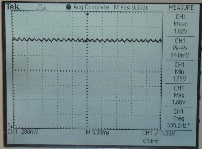
There is the driver running at 500mA

The voltage on the Fet's Gate oscillates as shown below

The mean gate voltage is 1.83V to control the led's current to 500mA with a 4.5V supply. The ripple (oscillation) is 0.136V peak to peak (pk-pk) but the frequency is 200Hz which is not visible to the eye. So the control is fine as it is.
However lets consider what we could do to improve the control and reduce the amplitude of this. In this discussion I am taking a practical approach to the problem rather then diving into the maths of sample data systems.
Lets consider:- i) the control, ii) input filtering, iv) output filtering, v) deadband, vi) proportional control, vii) variable gain/deadband
The ADC is sampling at about 5Ksamples/sec so it takes about 25 samples in each rise and fall of the trace. This means there are plenty of opportunities for the software to control the output so this is not the problem
The input anti-alias filter (R4, R5 and C4) slows down the
response of our control. A step change in the sensed current has to
charge up C4 before the ADC see the full effect. The time constant
for the input filter is about 3.1mS i.e. 1/(2*pi*C*R)Hz = 51Hz This
is fine as a filter for the sampling frequency of 5Ksamples/sec as
this gives a nyquist rate of 2.5Ksamples/sec, much higher then the
input filters cutoff. However the input filters' cutoff is well
below the 200Hz ripple frequency so the input filter is limiting the
controller's response to the changes in sense current (due to the
change in the Fet's gate voltage). This can be confirmed by reducing
C4 from 0.47uF to 0.1uF. (241Hz cutoff) This gives about 0.08V pk-pk
at about 430Hz. Going further and changing R3,R4 to 1.5K C4 0.1uF
(530Hz cutoff). The ripple is about 0.06V pk-pk and about 590Hz.
Actually the pk-pk and hz of all the measurements vary considerable.
The
disadvantage of increasing the frequency response of the input filter
is that it makes the system more sensitive to impulsive noise (noise
spikes).
The output of the controller is filtered by R2, C3. This RC filter turns the square wave (bangbang) output into a roughly smooth level for to drive the Fet gate. The RC time constant for this filter is about 47mS i.e. 3.3Hz. Increasing this time constant also reduces the ripple and increases the frequency. The disadvantage of increasing this time constant is that the response of the led becomes slower. It comes on and goes off slower. The advantage of a longer time constant is that the led is less responsive to noise spikes (flicker). These flickers become more noticeable at low light levels.
A deadband is often employed in bangbang controls to prevent cycling. As shown above the cycling is not significant at 500mA and can be further reduced if necessary without using deadband. But by all means experiment with putting some deadband into the code and investigate its effect.
Proportional control is another solution. Instead of switching the output on for full length of the ADC sample period, you could set a counter proportional to the size of the error and tri-state the output when the counter counts out. This would require taking the sleep out of the main loop and counting down the counter, or you could load one of the uC's counter/timers and handle the interrupt when it timed out. In either of these of these cases your ADC measurement will be noisier as the uC is running and switching outputs while the ADC is doing its conversion.
Because of the logarithmic response of the eye, low levels of light correspond to very low currents and hence very low ADC conversion counts (try a setpoint of 10 for example). At these levels you may need a different size of deadband or proportional gain, i.e. ones that vary with the current setpoint.
So there are a few ideas for you to try out. My preferred method for removing the flickering at low light levels is to have dual outputs with different time constants, similar to the circuit shown below.
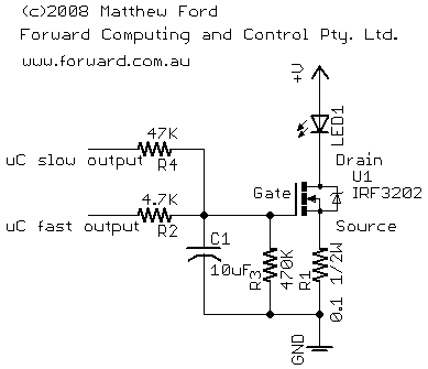
In this circuit the fast output is used to drive the led from one setpoint to another quickly, while the slow output is used to control the current at the setpoint without flickering.
The basic circuit can be used to control milliamps to amps. I have used it for a 5A led driver. The Power Fets used here (IRF3711 and IRL3202) can handle 110A and 20V drain to source and higher voltages are readily available. For higher powered torches you will probably want to increase both the supply voltage and the current.
The maximum current can be readily increased by reducing the sense resistor (R1 above). However the circuit as initially presented has a strict voltage limit of <6V maximum. This is set by the maximum voltage the uC can stand. To increase the supply current you will need to add a voltage regulator to supply the 5V to the uC.
There are many 3 terminal voltage regulators to choose from. Two low dropout / low power regulators I would suggest are:- LP2980 for up to 16V input and MIC5233 for upto 36V input. Note: these are both SMD devices. For a non-SMD device you can use an LM317 etc. for up to 40V input. Note that for a 5V supply the input voltage to the LM317 needs to be greater than 6.5V while the input voltage to the LP2980 and MIC5233 needs to be only greater then 5.25V (when supplying 50mA).
I received an email recently asking me for alternative FETs that could be used for this tutorial.
Almost any N-Channel FET in a TO-220 case can be used. The TO-220 case is used for high power, high current, low on resistance FETs. Because the FET is being used in a linear mode, the gate charge current specifications are not important and, for a supply of 5V or less, the various breakdown voltage specifications are not important either. The only thing you need to check is, that for the circuit's available gate drive voltage, that the voltage drop across the FET when it is passing 0.5A is low enough so that there is still enough voltage left to drive the LED. The circuit below shows the gate drive and the current path throught the led
The voltage supplied by the uC to the FET gate will be lower than the supply voltage due to the 4.7K + 47K resistor divider. This divider limits the maximum voltage at the FET gate to 0.91 times the uC Vcc voltage. That is about 3.3V for a 3.6V supply (i.e. 3 x NiMH batteries).
The voltage available to the drive the Led is the supply voltage
less the voltage drop across the FET (Vds) and the voltage drop
across the current sense resistor 0.1 ohm. At 0.5A, the voltage
across the sense resistor is 0.05V so the Led voltage is
Led V
= Vcc - 0.05V - Vds (FET)
The K2 Led I am using here typically needs about 3.5V to pass 0.5A (see graph below). However you should note that this Led current to voltage curve varies from Led to Led and varies with temperature.

Fig 1. K2 typical I versus V curve
So for a typical K2 Led, with a 3.6V supply, we want the FET (Vds)
to be less than 0.1V
Led V = 3.6 - 0.05 - 0.1 = 3.45V.
and the
available gate drive voltage (Vgs) is 3.3V
To check that the Vds for the FET at a given gate voltage, in the FET datasheet look for the graph of Drain to Source Current (Id) versus Drain to Source Voltage (Vds) for various gate voltages (Vgs).
Below is the graph for the FET listed in the tutorial, IRF3202. With a 2.5V gate drive this FET will pass 5A with less than 0.1V drop. At 0.5A the voltage drop will be about 10 times less or 0.01V. This is a very good FET for this application

Fig 2. IRF3202
For comparison here is an example of a FET that not as good but still very usable, IRLZ24N. With a 3V gate drive this FET will pass 0.7A with less than 0.1V drop.

Fig 3. IRLZ24N
Finally here is an example of a FET you would NOT want to use, IRFB4620

Fig 4. IRFB4620 – Do not use
Even with a gate drive of 5V (Vgs), the voltage drop across the
IRFB4620 is about 3V (Vds) at 300mA (Id). If you used this FET the
led may glow but not very brightly and you would not be able to drive
it at 500mA even if you used a 5V supply.
Don't use more than
a 5V supply or you will destroy the Attiny84 uC.

Contact Forward Computing and Control by
©Copyright 1996-2020 Forward Computing and Control Pty. Ltd.
ACN 003 669 994